Integrated Transceiver-Based 3D Sensing Using Dispersion Metasurfaces
It features a transmitting metasurface generating chromatic line focuses as depth markers and a symmetrically arranged receiving metasurface.
CHENGDU, SICHUAN, CHINA, July 9, 2025 /EINPresswire.com/ -- Check out the full article here: https://www.oejournal.org/oea/article/doi/10.29026/oea.2025.240299Optical three-dimensional (3D) measurement plays a vital role in various fields such as intelligent manufacturing and biomedical engineering, particularly in high-precision inspection and the reconstruction of complex structures. Current 3D measurement techniques are broadly categorized into interferometric and non-interferometric approaches. Interferometric methods, such as shear interferometry and white-light interferometry, are widely applied in nanometer-scale metrology and precision manufacturing due to their superior depth resolution. However, these techniques often rely on complex optical setups composed of numerous bulk optical components, resulting in bulky systems with high environmental stability requirements, thereby limiting their suitability for real-time, in-line measurement applications.
In contrast, non-interferometric methods—such as structured light and light field techniques—offer greater flexibility by reducing dependence on traditional optical hardware through system-level optimization of optical elements and reconstruction algorithms. Nevertheless, this increased integration often comes at the cost of higher optical design complexity and computational burden. Consequently, achieving high precision while simplifying system design and enhancing measurement efficiency remains a central challenge in the field of optical 3D sensing.
Metasurfaces, with their unique advantages in arbitrary wavefront control, planar configuration, and ease of integration, have recently gained significant attention in the development of compact, multifunctional, and high-performance 3D optical systems. However, limitations in the design and fabrication accuracy of current nanostructures still hinder the efficiency and imaging quality of metasurfaces. Furthermore, when measuring high-refractive-index surfaces, strong reflections and multiple scattering events introduce substantial challenges for active imaging approaches, making it difficult to achieve high-accuracy measurements in complex environments. Existing studies primarily focus on demonstrating the functional capabilities of metasurfaces, rather than developing integrated detection devices. Therefore, leveraging the flexible design capabilities of metasurfaces to enhance their adaptability and robustness in complex imaging scenarios—while realizing compact, integrated detection systems—remains a crucial direction for metasurface-enabled 3D sensing.
A collaborative research effort between Professor Lingling Huang’s team at Beijing Institute of Technology and Professor Rui You’s team at Beijing Information Science and Technology University has demonstrated a single-layer, monolithic optical metasystem capable of three-dimensional inspection of fine structural features. This system integrates both transmission and reception functionalities into a compact metasurface architecture. The emitting metasurface utilizes off-axis longitudinal dispersion characteristics to focus broadband illumination into a series of discrete focal points. Symmetrically arranged, the receiving metasurface is designed to selectively collect reflected light from in-focus regions while effectively suppressing out-of-focus noise signals.
To enable efficient depth extraction, the team developed a fast and lightweight reconstruction algorithm based on a monotonic and continuous spectral-to-depth mapping strategy, allowing precise retrieval of 3D structural information. The system demonstrates the ability to accurately reconstruct depth variations as fine as 20 µm, while maintaining lateral resolution errors under 10 µm. This technology holds great promise for applications in industrial inspection, semiconductor manufacturing, and biomedical engineering. The results were published in Opto-Electronic Advances, Issue 8, 2025, under the title “Three-dimensional Measurement Enabled by Single-layer All-in-one Transmitting-receipting Optical Metasystem.”
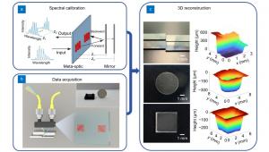
As illustrated in Figure 1, the schematic of the proposed 3D measurement system shows that when a broadband light source is incident upon Metasurface 1 (MS1), its off-axis dispersive metalens properties cause different wavelengths to focus at distinct depths. Upon illuminating a target with 3D topography, the reflected light is captured by the symmetrically positioned Metasurface 2 (MS2) and exits through its output ports. After data acquisition, a lightweight point-wise reconstruction algorithm analyzes the spectral data to retrieve precise height information at each spatial point, ultimately reconstructing the full 3D profile of the target object. Owing to its compact light source and detector integration, as well as its fast computational capabilities, the proposed all-in-one metasurface optical system offers excellent adaptability across various inspection scenarios and measurement environments.
Following the overall measurement workflow, the research team conducted a series of 3D sensing and reconstruction experiments on various materials and objects. As shown in Fig. 2(a), prior to measurement, a spectral-to-depth calibration was performed to establish a correspondence matrix between reflected spectral signals and depth positions. This was achieved by translating a reference mirror along the optical axis and recording the reflected spectra at different depths. After completing the calibration process, the team acquired reflection spectra from the target object, as illustrated in Fig. 2(b). The spectral data were then processed using the reconstruction algorithm to generate the 3D profile of the object, as presented in Fig. 2(c).
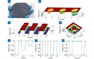
The system's adaptability was verified through successful 3D reconstruction of metallic samples and silicon wafers. Furthermore, the team applied the system to scan and reconstruct structures of varying dimensions fabricated on semiconductor wafers. As shown in Fig. 3, the results confirm that the system achieves a depth resolution of ±20 μm and a lateral accuracy of ±10 μm, demonstrating its effectiveness in precise surface profiling across different material types.
This collaborative research was conducted by the Laboratory of Nanophotonics and Novel Display, Beijing Institute of Technology, and the Laboratory of Intelligent Microsystems at Beijing Information Science and Technology University. The research teams focus on a wide range of topics, including the physical mechanisms and functional applications of novel micro/nano-optical components, light field manipulation, diffractive optics, holography, information optics, emerging display principles and devices, as well as nano-optoelectronic functional materials and devices. Professors Lingling Huang and Rui You are the corresponding authors of this work.
This research was supported by the National Key R&D Program of China (2021YFA1401200), the Beijing Outstanding Young Scientist Program (BJJWZYJH01201910007022), the National Natural Science Foundation of China (U21A20140, 92050117,62105024), and the Beijing Distinguished Young Scholar Program (JQ24028).
Andrew Smith
Charlesworth
+ +44 7753 374162
marketing@charlesworth-group.com
Visit us on social media:
LinkedIn
YouTube
Other
Distribution channels: Book Publishing Industry, Electronics Industry, Science, Technology, Telecommunications
Legal Disclaimer:
EIN Presswire provides this news content "as is" without warranty of any kind. We do not accept any responsibility or liability for the accuracy, content, images, videos, licenses, completeness, legality, or reliability of the information contained in this article. If you have any complaints or copyright issues related to this article, kindly contact the author above.
Submit your press release


